Introduction
I’ve been looking into some projects involving an LED matrix; but hit a few road blocks due to issues with the sheer number of LEDs I need to control. I’ve always known about the existence of shift registers and their ability to control many LEDs and other components without needing separate pins to drive each small bit of my circuits, so I thought I’d look into how they work.
I picked up a kit recently that had a SN74HC595N Shift Register in it, and with a bit of help from the datasheet I was able to begin working on some projects with it.
Understanding Shift Registers
A shift register is a device that accepts a stream of serial bits and simultaneously output the values of those bits onto parallel I/O pins. They come in handy when trying to drive a large numbers of LEDs or basically any other component that might require a vast number of outputs. The diagram below illustrates all the various inputs and outputs available on a standard shift register IC.
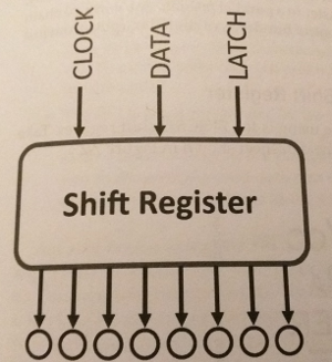
The inputs are made up of three serial communication lines that connect to the shift register from the Arduino. The eight circles represent LEDs connected to eight outputs of the shift register.
Say you wanted sufficient data to control eight LEDs digitally; you’d need to find a way to transmit 8 total bits of information where each bit represented a high on an LED. If we wanted to turn on eight LEDs with eight digital outputs; all the bits would be transmitted on independent I/O pins.
We are going to be focusing on serial in, parallel out (SIPO) shift registers. These devices allow us to clock in multiple bytes of data serially, and output them from the shift register all at once in a parallel fashion.
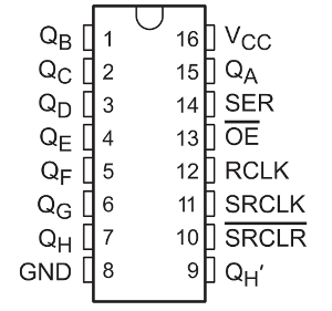
Take a look at the pin-out diagram for our Shift register below
-
Q(A) -> Q(H)- Represent the eight parallel outputs from the shift register. These are the same outputs shown in the first diagram. -
VCC- Connected to 5V -
GND- Shared grounding pin -
SER- The equivalent of theDATA pinshown in the first diagram. This is the pin where you will feed in the eight sequential bit values to set the values of the parallel output. -
SRCLK- The equivalent of theCLOCK pinshown in the first diagram. Every time the pin goes high, the values in the shift register shift by 1 bit. It will be pulsed eight times to pull in all the data that you are sending on the data pin. -
RCLK- The equivalent of theLATCH pinshown in the first diagram. Also known as theregister clock pin, the latch pin is used tocommitthe recently shifted serial values to the parallel outputs all at once. This pins allows you to sequentially shift data into the chip and have all the values show up on the parallel outputs at the same time. -
OE- Output Enable, the bar over the top indicates that is active low; meaning that when the pin is held low, the output will be enabled. When it is high the output will be disabled. -
SRCLR- Serial Clear pin, again the bar means that is is also an active low. When pulled low, it empties the contents of the shift register.
How the Shift Register works
A shift register is a synchronous device; it only acts on the rising edge of the clock signal. Every time the clock signal transitions from low to high, all the values currently stored in the eight output registers are shifted over one position (the last one is either discarded or output on the Q(H)' pin if you are cascading registers).
Simultaneously, the value currently on the DATA input is shifted into the first position. By doing this eight times, the present values are shifted out and the new values are shifted into the register. The LATCH pin is set high at the end of the cycle to make the newly shifted values appear on the outputs.
Below depicts the process we would take if we wanted to set every other LED to the ON state (Q(A), Q(C), Q(E), Q(G)). Represented in binary, we want the output of the parallel pins on the shift register to look like this: 10101010.
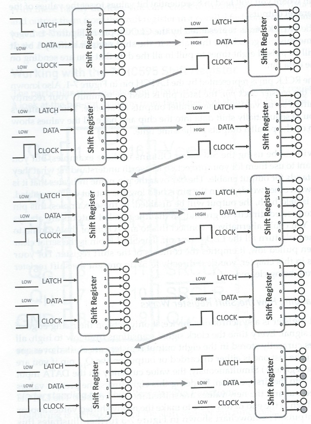
First, the LATCH pin is set low so that the current LED states are not changed while new values are shifted in. Then, the LED states are shifted into the registers in order on the CLOCK edge from the DATA line. After all the values have been shifted in, the LATCH pin is set high again, and the values are outputted from the shift registers.
Shifting Serial Data from the Arduino
Now that we understand how the Shift Register works, we can write Arduino code to control the shift register. Luckily there is already a library for controlling this type of system called shiftOut.
shiftOut() is setup to shift out a byte of data at a time. It can be told to start shifting from either the most or least significant bit and uses the following syntax with the listed arguments:
shiftOut(dataPin, clockPin, bitOrder, value)-
dataPin- Specifies the data pin (SER) number -
clockPin- Specifies the clock pin (SRCLK) number -
bitOrder- Set to either MSBFIRST or LSBFIRST to define what order we want the bits read into the shift register -
value- The value to shift out. If you are feeding in a binary number similar to the example above; it must be prefixed with a capitalBin order to alert the Arduino IDE to interpret the following numbers as binary rather than an integer.eg. B10101010
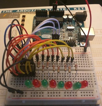
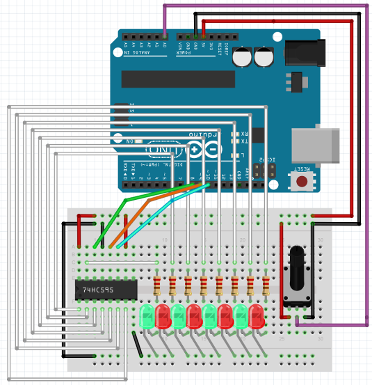
Using this knowledge I went about setting up my circuit. The goal was to have eight LEDs controlled by our three pin inputs and have them display in binary; the numbers 0-255. Refer to my circuit diagram below for details on the circuit design.
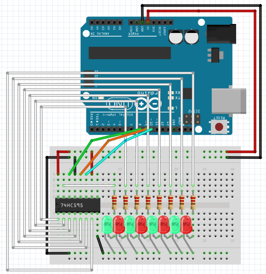
Once you’ve wired up your circuit you’ll have something that will look at little bit like the following (yours will probably be neater than mine).
The Code
The code is actually super easy; We start with our pin constants along with a variable to store the current value we’re inserting into the LED
const int SER = 8; // Serial output to shift register
const int LATCH = 9; // Shift register latch pin
const int CLK = 10; // Shift register clock pin

int value = 0; // Value to display
Next in the setup() we specify our pinModes
pinMode(SER, OUTPUT);
pinMode(LATCH, OUTPUT);
pinMode(CLK, OUTPUT);
Then we move down into the loop() and add first hold the LATCH pin low to start feeding our value into the shift register
digitalWrite(LATCH, LOW); // Latch lowNow we use the shiftOut() function to push our value into the shift register. NOTE that the spelling of value should match the value we declared earlier on.
shiftOut(SER, CLK, LSBFIRST, value); // Shift most sig. bit firstFinally we set the LATCH to high and push the loaded value our of the shift registers pins to light up the LEDs
digitalWrite(LATCH, HIGH); // Latch high, show patternIf you run the code now, you should get no LEDs lighting up. This is because we are passing in a value of 0 (as declared in the value variable); so lets go ahead and create a method of cycling from all the different numbers that we can represent in binary on our LEDs.
The following code will increment the value of value by 1 each time the Shift register latches. If the value reaches 255, it resets back to 0 and continues.
// check value is less than the 255 limit and reset if it isn't
if(value < 255)
{
    value++;
}
else
{
  value = 0;
}
It it also worth adding in some delay code so that we can actually see the changes occurring
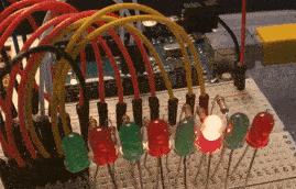
delay(100);Lets run the code!
Expand on ideas
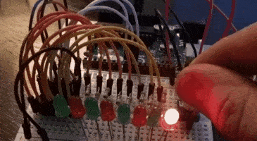
With what we now know, we can do some pretty cool things. Another idea I went ahead and implemented was a potentiometer controlled bar that will light up as the value extracted from the potentiometer increases.
I used the Shift register circuit we built plus a simple potentiometer input. I’ve included the code and some pictures below that outline my design.
const int SER = 8; // Serial output to shift register
const int LATCH = 9; // Shift register latch pin
const int CLK = 10; // Shift register clock pin

const int IN = A0; // Input from potentiometer

int potentLow = 0;
int potentHigh = 1024;

void setup() {
  pinMode(SER, OUTPUT);
  pinMode(LATCH, OUTPUT);
  pinMode(CLK, OUTPUT);
}

void loop() {
  int value = analogRead(IN);

  // Level out highs and low inputs
  if (value > potentHigh){
    potentHigh = value;
  }
  if (value < potentLow){
    potentLow = value;
  }

  // Map output values between 0 and 255
  int valueOut = map(value,potentLow,potentHigh, 0, 255);

  // Statically set output value based on input constraints
  if(value <= 32){valueOut = 1;}
  if(value > 32 && value <= 64){valueOut = 3;}
  if(value > 64 && value <= 96){valueOut = 7;}
  if(value > 96 && value <= 128){valueOut = 15;}
  if(value > 128 && value <= 160){valueOut = 31;}
  if(value > 160 && value <= 192){valueOut = 63;}
  if(value > 192 && value <= 224){valueOut = 127;}
  if(value > 224){valueOut = 255;}

  digitalWrite(LATCH, LOW); // Latch low
  shiftOut(SER, CLK, LSBFIRST, valueOut); // Shift most sig. bit first
  digitalWrite(LATCH, HIGH); // Latch high, show pattern

  delay(10);
}
Conclusion
Shift Registers are very powerful when used in the right places. They can be changed together allowing expansion outwards from 8bit to as many Shift Registers as required. Overall this project was a really interesting look into what is available and has given me a lot of really interesting ideas for future projects.
I would love to hear what projects you’ve used Shift registers for in the past; or even what you plan to do with them in the future!